Marknadens största urval
Snabb leverans

Böcker i Woodhead Publishing Series in Electronic and Optical Materials-serien

Filter
Filter
Sortera efterSortera Serieföljd
  • av Virginia, Va, Virginia Tech, m.fl.
    3 479,-

    The need to more efficiently harvest energy for electronics has spurred investigation into materials that can harvest energy from locally abundant sources. Ferroelectric Materials for Energy Harvesting and Storage is the first book to bring together fundamental mechanisms for harvesting various abundant energy sources using ferroelectric and piezoelectric materials. The authors discuss strategies of designing materials for efficiently harvesting energy sources like solar, wind, wave, temperature fluctuations, mechanical vibrations, biomechanical motion, and stray magnetic fields. In addition, concepts of the high density energy storage using ferroelectric materials is explored. Ferroelectric Materials for Energy Harvesting and Storage is appropriate for those working in materials science and engineering, physics, chemistry and electrical engineering disciplines.Reviews wide range of energy harvesting including solar, wind, biomechanical and moreDiscusses ferroelectric materials and their application to high energy density capacitorsIncludes review of fundamental mechanisms of energy harvesting and energy solutions, their design and current applications, and future trends and challenges

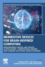
  • - From Materials, Devices, and Circuits to Applications Computational Memory, Deep Learning, and Spiking Neural Networks
     
    3 675,-

  • - Architectures, Protocols, Operation and Deployment
     
    2 759,-

    Part one covers architectures for VCS, part two describes the physical layer, antenna technologies and propagation models, part three explores protocols, algorithms, routing and information dissemination and part four looks at the operation and deployment of vehicular communications and networks.

  •  
    3 295,-

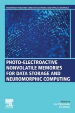
    Photo-Electroactive Non-Volatile Memories for Data Storage and Neuromorphic Computing summarizes advances in the development of photo-electroactive memories and neuromorphic computing systems, suggests possible solutions to the challenges of device design, and evaluates the prospects for commercial applications. Sections covers developments in electro-photoactive memory, and photonic neuromorphic and in-memory computing, including discussions on design concepts, operation principles and basic storage mechanism of optoelectronic memory devices, potential materials from organic molecules,  semiconductor quantum dots to two-dimensional materials with desirable electrical and optical properties, device challenges, and possible strategies.  This comprehensive, accessible and up-to-date book will be of particular interest to graduate students and researchers in solid-state electronics. It is an invaluable systematic introduction to the memory characteristics, operation principles and storage mechanisms of the latest reported electro-photoactive memory devices. Reviews the most promising materials to enable emerging computing memory and data storage devices, including one- and two-dimensional materials, metal oxides, semiconductors, organic materials, and moreDiscusses fundamental mechanisms and design strategies for two- and three-terminal device structuresAddresses device challenges and strategies to enable translation of optical and optoelectronic technologies

  • - Investigation of Ferroelectric, Dielectric, and Semiconductor Materials and Devices
    av Yasuo (Tohoku University Cho
    2 925,-

    Scanning Nonlinear Dielectric Microscopy: Investigation of Ferroelectric, Dielectric, and Semiconductor Materials and Devices is the definitive reference on an important tool to characterize ferroelectric, dielectric and semiconductor materials. Written by the inventor, the book reviews the methods for applying the technique to key materials applications, including the measurement of ferroelectric materials at the atomic scale and the visualization and measurement of semiconductor materials and devices at a high level of sensitivity. Finally, the book reviews new insights this technique has given to material and device physics in ferroelectric and semiconductor materials. The book is appropriate for those involved in the development of ferroelectric, dielectric and semiconductor materials devices in academia and industry. Presents an in-depth look at the SNDM materials characterization technique by its inventorReviews key materials applications, such as measurement of ferroelectric materials at the nanoscale and measurement of semiconductor materials and devicesAnalyzes key insights on semiconductor materials and device physics derived from the SNDM technique

  •  
    3 125,-

    Spectroscopy of Lanthanide Doped Oxide Materials provides a comprehensive overview on the most essential characterization techniques of these materials, along with their key applications. The book describes the application of optical spectroscopy of lanthanides doped inorganic phosphor hosts and gives information about their structure and morphology, binding energies, energy of transition and band gap. Also discussed are the properties and applications of rare earth doped inorganic materials and the barriers and potential solutions to enable the commercial realization of phosphors in important applications. The book reviews key information for those entering the field of phosphor research, along with the fundamental knowledge of the properties of transition series elements under UV/Visible/NIR light exposer. Low-cost materials methods to synthesize the materials and spectroscopic characterization methods are also detailed.Reviews the barriers and potential solutions to enable commercial realization of inorganic phosphorsDiscusses low-cost material methods to synthesize and characterize lanthanide doped oxide materialsProvides readers with a comprehensive overview on key properties for the most relevant applications, such as lighting and display, energy conversion and solar cell devices

  • - Materials, Properties and Devices
     
    3 125,-

    Ferroelectricity in Doped Hafnium Oxide: Materials, Properties and Devices covers all aspects relating to the structural and electrical properties of HfO2 and its implementation into semiconductor devices, including a comparison to standard ferroelectric materials. The ferroelectric and field-induced ferroelectric properties of HfO2-based films are considered promising for various applications, including non-volatile memories, negative capacitance field-effect-transistors, energy storage, harvesting, and solid-state cooling. Fundamentals of ferroelectric and piezoelectric properties, HfO2 processes, and the impact of dopants on ferroelectric properties are also extensively discussed in the book, along with phase transition, switching kinetics, epitaxial growth, thickness scaling, and more. Additional chapters consider the modeling of ferroelectric phase transformation, structural characterization, and the differences and similarities between HFO2 and standard ferroelectric materials. Finally, HfO2 based devices are summarized.Explores all aspects of the structural and electrical properties of HfO2, including processes, modelling and implementation into semiconductor devicesConsiders potential applications including FeCaps, FeFETs, NCFETs, FTJs and moreProvides comparison of an emerging ferroelectric material to conventional ferroelectric materials with insights to the problems of downscaling that conventional ferroelectrics face

  • - Fibre Types, Materials, Fabrication, Characterisation and Applications
     
    3 089,-

  • - Systems and Applications
     
    3 529,-

  •  
    2 135,-

    The directed self-assembly (DSA) method of patterning for microelectronics uses polymer phase-separation to generate features of less than 20nm, with the positions of self-assembling materials externally guided into the desired pattern. Directed self-assembly of Block Co-polymers for Nano-manufacturing reviews the design, production, applications and future developments needed to facilitate the widescale adoption of this promising technology. Beginning with a solid overview of the physics and chemistry of block copolymer (BCP) materials, Part 1 covers the synthesis of new materials and new processing methods for DSA. Part 2 then goes on to outline the key modelling and characterization principles of DSA, reviewing templates and patterning using topographical and chemically modified surfaces, line edge roughness and dimensional control, x-ray scattering for characterization, and nanoscale driven assembly. Finally, Part 3 discusses application areas and related issues for DSA in nano-manufacturing, including for basic logic circuit design, the inverse DSA problem, design decomposition and the modelling and analysis of large scale, template self-assembly manufacturing techniques.

  • - Materials, Devices and Applications
    av Philadelphia, USA) Nabet & Bahram (Drexel University
    2 609,-

  • - Monitoring, Control and Automation
     
    2 809,-

  • - Design, Synthesis, Properties and Applications
     
    2 815,-

    Magnetic nanowires and microwires are key tools in the development of enhanced devices for information technology (memory and data processing) and sensing. Offering the combined characteristics of high density, high speed, and non-volatility, they facilitate reliable control of the motion of magnetic domain walls; a key requirement for the development of novel classes of logic and storage devices. Part One introduces the design and synthesis of magnetic nanowires and microwires, reviewing the growth and processing of nanowires and nanowire heterostructures using such methods as sol-gel and electrodeposition combinations, focused-electron/ion-beam-induced deposition, chemical vapour transport, quenching and drawing and magnetic interactions. Magnetic and transport properties, alongside domain walls, in nano- and microwires are then explored in Part Two, before Part Three goes on to explore a wide range of applications for magnetic nano- and microwire devices, including memory, microwave and electrochemical applications, in addition to thermal spin polarization and configuration, magnetocalorific effects and Bloch point dynamics. Detailed coverage of multiple key techniques for the growth and processing of nanowires and microwiresReviews the principles and difficulties involved in applying magnetic nano- and microwires to a wide range of applicationsCombines the expertise of specialists from around the globe to give a broad overview of current and future trends

  • - Materials, Structures, and Applications
    av Gopalan (Oakland University) Srinivasan, Shashank (Pennsylvania State University Priya & Nian (Northeastern University Sun
    2 265,-

    The first part of the book gives the reader a summary of the theory behind magnetoelectric phenomena, it then introduces magnetoelectric materials and structures and the techniques used to fabricate and characterise them. Part two looks at magnetoelectric devices.

  • - Materials, Synthesis, Characterization and Applications
     
    3 249,-

  • - Technologies, Social Impact and Sustainability
    av N. Saito & D. Menga
    2 809,-

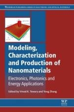
  • - Electronics, Photonics and Energy Applications
     
    3 249,-

    Part one covers modeling techniques incorporating quantum mechanical effects to simulate nanomaterials and devices. Part two describes the characterization of nanomaterials using diffraction techniques and Raman spectroscopy. Part three looks at the structure and properties of nanomaterials. Part four explores nanofabrication and nanodevices.

  • av Andrew S. (Voxtel Inc Huntington
    3 295,-

  • av E-H Wong
    2 579,-

    Failure of electronic packaging: Effects of temperature, moisture and mechanical driving forces provides a thorough review of this important field of research.

  • - Design, Synthesis, Properties and Applications
     
    5 049,-

    Magnetic Nano-and Microwires: Design, Synthesis, Properties and Applications, Second Edition, reviews the growth and processing of nanowires and nanowire heterostructures using such methods as sol-gel and electrodeposition, focused-electron/ion-beam-induced deposition, epitaxial growth by chemical vapor transport, and more. Other sections cover engineering nanoporous anodic alumina, discuss magnetic and transport properties, domains, domain walls in nano-and microwires. and provide updates on skyrmions, domain walls, magnetism and transport, and the latest techniques to characterize and analyze these effects. Final sections cover applications, both current and emerging, and new chapters on memory, sensor, thermoelectric and nanorobotics applications. This book will be an ideal resource for academics and industry professionals working in the disciplines of materials science, physics, chemistry, electrical and electronic engineering and nanoscience. Details the multiple key techniques for the growth, processing and characterization of nanowires and microwiresReviews the principles and difficulties involved in applying magnetic nano- and microwires to a wide range of applications, also including biomedical and sensing applicationsDiscusses magnetism and transport in nanowires, skyrmions and domain walls in nanowires and the latest innovations in magnetic imaging


  • - Materials, Devices, and Applications
     
    4 119,-

  • av Hengyun (Shanghai University of Engineering Science Zhang
    3 479,-

  • - Fundamentals, Designs, and Applications
     
    3 109,-

    Dielectric Metamaterials: Fundamentals, Designs, and Applications links fundamental Mie scattering theory with the latest dielectric metamaterial research, providing a valuable reference for new and experienced researchers in the field. The book begins with a historical, evolving overview of Mie scattering theory. Next, the authors describe how to apply Mie theory to analytically solve the scattering of electromagnetic waves by subwavelength particles. Later chapters focus on Mie resonator-based metamaterials, starting with microwaves where particles are much smaller than the free space wavelengths. In addition, several chapters focus on wave-front engineering using dielectric metasurfaces and the nonlinear optical effects, spontaneous emission manipulation, active devices, and 3D effective media using dielectric metamaterials. Highlights a crucial link in fundamental Mie scattering theory with the latest dielectric metamaterial research spanning materials, design and applicationsIncludes coverage of wave-front engineering and 3D metamaterialsProvides computational codes for calculating and simulating Mie resonances

  •  
    3 309,-

    Fundamentals and Sensing Applications of 2D Materials provides a comprehensive understanding of a wide range of 2D materials. Examples of fundamental topics include: defect and vacancy engineering, doping and advantages of 2D materials for sensing, 2D materials and composites for sensing, and 2D materials in biosystems. A wide range of applications are addressed, such as gas sensors based on 2D materials, electrochemical glucose sensors, biosensors (enzymatic and non-enzymatic), and printed, stretchable, wearable and flexible biosensors. Due to their sub-nanometer thickness, 2D materials have a high packing density, thus making them suitable for the fabrication of thin film based sensor devices. Benefiting from their unique physical and chemical properties (e.g. strong mechanical strength, high surface area, unparalleled thermal conductivity, remarkable biocompatibility and ease of functionalization), 2D layered nanomaterials have shown great potential in designing high performance sensor devices. Provides a comprehensive overview of 2D materials systems that are relevant to sensing, including transition metal dichalcogenides, metal oxides, graphene and other 2D materials systemIncludes information on potential applications, such as flexible sensors, biosensors, optical sensors, electrochemical sensors, and more Discusses graphene in terms of the lessons learned from this material for sensing applications and how these lessons can be applied to other 2D materials

  • - Fundamentals and Applications of CMOS and CCD Sensors
     
    3 675,-

    High Performance Silicon Imaging: Fundamentals and Applications of CMOS and CCD Sensors, Second Edition, covers the fundamentals of silicon image sensors, addressing existing performance issues and current and emerging solutions. Silicon imaging is a fast growing area of the semiconductor industry. Its use in cell phone cameras is already well established, with emerging applications including web, security, automotive and digital cinema cameras. The book has been revised to reflect the latest state-of-the art developments in the field, including 3D imaging, advances in achieving lower signal noise, and new applications for consumer markets. The fundamentals section has also been expanded to include a chapter on the characterization and testing of CMOS and CCD sensors that is crucial to the success of new applications. This book is an excellent resource for both academics and engineers working in the optics, photonics, semiconductor and electronics industries.Covers the fundamentals of silicon-based image sensors and technical advances, focusing on performance issuesLooks at image sensors in applications, such as mobile phones, scientific imaging, and TV broadcasting, and in automotive, consumer and biomedical applicationsAddresses the theory behind 3D imaging and 3D sensor development, including challenges and opportunities

Gör som tusentals andra bokälskare

Prenumerera på vårt nyhetsbrev för att få fantastiska erbjudanden och inspiration för din nästa läsning.